Optical spectroscopy is a common tool with several applications at various stages of production in semiconductor manufacturing. The benefit of Avantes’ modular fiber optic based spectrometers is the ability to facilitate in situ measurements within production environments, providing near real-time measurements without disrupting manufacturing processes.
Plasma Diagnostics and End Point Detection with Spectroscopy

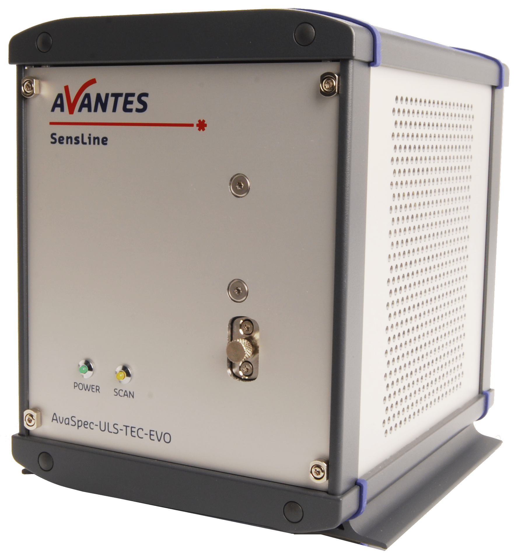
Plasma is the fourth state of matter after solid, liquid, and gas and is one of the most common states of matter in the universe, for example, our Sun is a giant ball of plasma. Plasma is a gas in which a large percentage of the atoms have been ionized through the application of energy, often in the form of electromagnetic current. The atoms excited this way must discharge their energy and one common way they do so is by emitting light. Because each element has a known spectroscopic profile, it is possible to closely monitor the atomic chemical makeup of a plasma reaction. It is also important to detect changes in the reaction phase and reaction endpoint. Measuring such a dynamic matrix requires high-speed data acquisition and high-resolution spectroscopic sampling achievable with the AvaSpec-ULS2048L-EVO spectrometer or for even greater resolution the 4096 pixel AvaSpec-ULS4096CL-EVO.
Plasma enhanced chemical vapor deposition (PECVD) uses plasma generated by applying electric current to a reactant gas vapor causing a chemical reaction that in turn grows deposits on a solid substrate to form a thin film. The properties and quality of this thin film are entirely dependent on the chemical reaction taking place. This is an elemental process in the manufacturing of semiconductors but generating a plasma and the chemical vapor deposition process require an air-tight vacuum chamber amid chemical vapors that must be maintained at the correct concentrations. Getting real-time measurements under these conditions are impossible for many measurement techniques and monitoring methods that might work elsewhere.
Fiber-optic-based spectroscopy, with the help of a vacuum feed-through attachment, allows stand-off measurements virtually in real time for these challenging test environments. With Avantes’ rEVOlutionary micro-processing package featuring Ethernet capability, that stand-off distance is nearly limitless.
Spectroscopy Thin Film Measurements
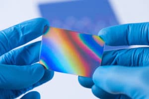
During and after the deposition coating process, properties of the deposited film will be characterized and validated using reflection and/or transmission actual thin film measurements can be compared against known optical constants of the substrate and materials used in the coating process. The AvaSoft-ThinFilm module is equipped for single-layer thin film measurements on films ranging from 10 nm to 50 µm in thickness with 1 nm resolution, available with optional onboard reference standards for selected coated and uncoated substrates for validation. For measurements of films greater than 50 µm in thickness or for multiple layers, discuss data analysis options with your sales engineer.
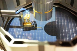
Wafer Probing and Inspection
The finished semiconductor wafers require quality control inspections and wafer probing with spectroscopy allows very high-speed testing of minute areas as small as 500-100 microns. At this stage of semiconductor manufacturing, the resolution is not as critical as production through-put, placing the focus on data acquisition and transmission speed. Avantes Evo series spectrometers provide the advantage of ultra-fast USB3 communications and the onboard processing power of the Xilinx Zinq 7010 microprocessor for speed and efficiency.
Avantes Spectrometers for the Semiconductor Industry
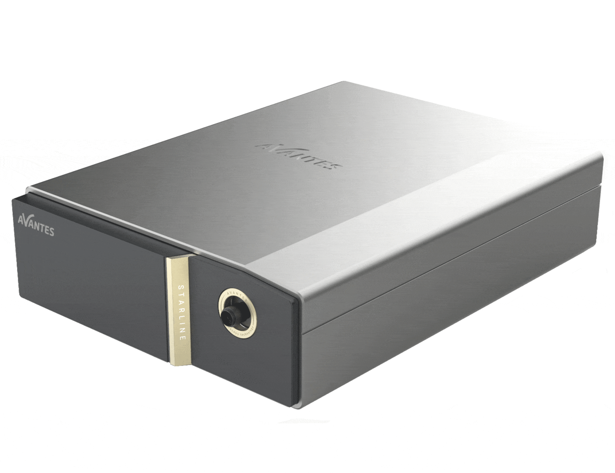
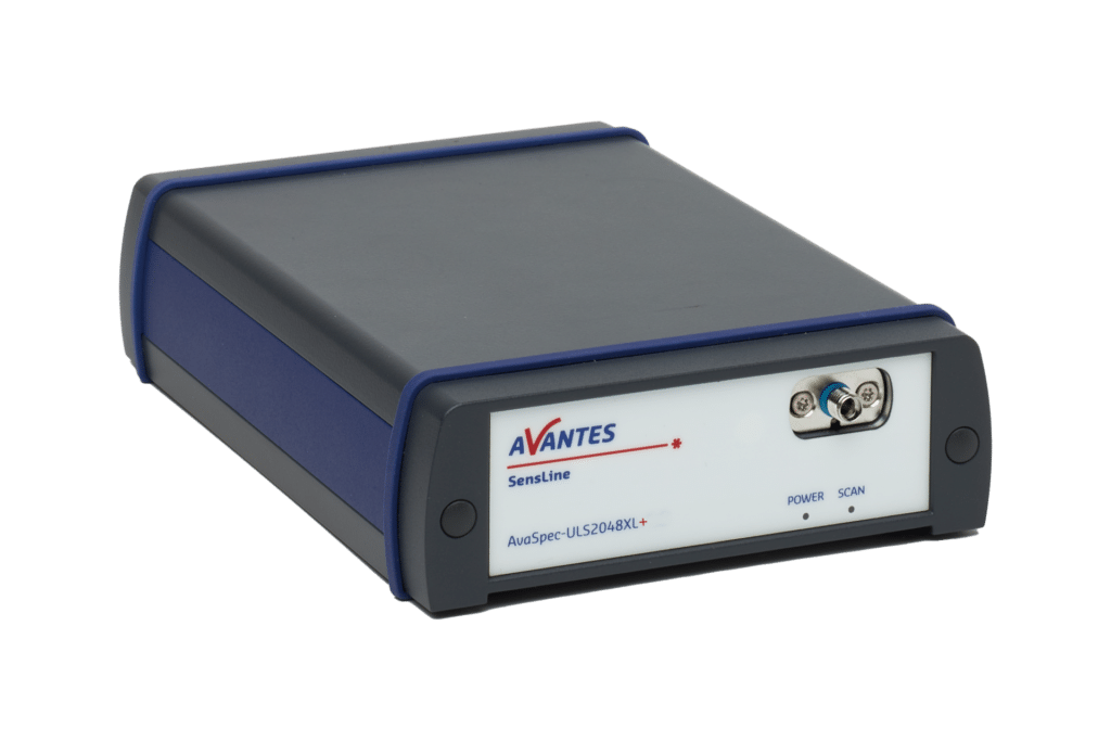
In Avantes’ two decades in spectroscopy, we have deployed our systems in hundreds of applications. Our instruments are available as desktop instruments in modular single channel housings or as the multi-channel rack mount style housing favored by original equipment manufacturers
Why Avantes for your Semiconductor application?
- High resolution (0.1 nm FWHM or better) spectral data collection for optical emission spectroscopy applications such as endpoint detection
- High-speed measurement capability (in milliseconds) for wafer probing throughput
- Ability to support thin film measurement applications with a broadband instrument configuration covering 360-1100 and 200-1100 nm.
- Growing selection of updated CMOS array instruments for optimal SWIR measurements (800-1100 nm) of coatings.
- Affordable NIR spectrometer options with high speed, low noise electronics
 My Cart
